Experiments-3
Construction of half/ full adder using XOR and NAND gates and verification of its operation
Introduction
Adders are digital circuits that carry out addition of numbers. Adders are a key component of arithmetic logic unit. Adders can be constructed for most of the numerical representations like Binary Coded Decimal (BCD), Excess – 3, Gray code, Binary etc. out of these, binary addition is the most frequently performed task by most common adders. Apart from addition, adders are also used in certain digital applications like table index calculation, address decoding etc.
Binary addition is similar to that of decimal addition. Some basic binary additions are shown below.
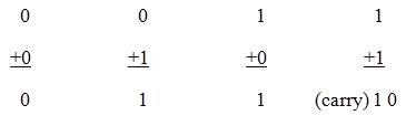
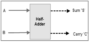
Figure 1. Schematic representation of half adder
1)Half Adder
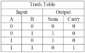
Half adder is a combinational circuit that performs simple addition of two binary numbers. If we assume A and B as the two bits whose addition is to be performed,the block diagram and a truth table for half adder with A, B as inputs and Sum, Carry as outputs can be tabulated as follows.
The sum output of the binary addition carried out above is similar to that of an Ex-OR operation while the carry output is similar to that of an AND operation. The same can be verified with help of Karnaugh Map.
The truth table and K Map simplification and logic diagram for sum output is shown below.
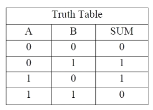
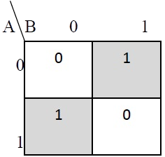
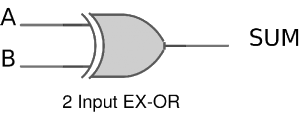
Figure 3. Truth table, K Map simplification and Logic diagram for sum output of half adder
The truth table and K Map simplification and logic diagram for carry is shown below.
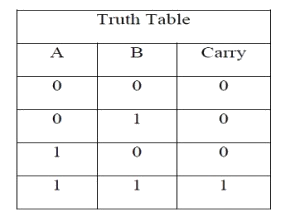
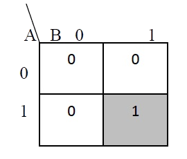
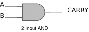
Figure 4. Truth table, K Map simplification and Logic diagram for sum output of half adder
Carry = AB
If A and B are binary inputs to the half adder, then the logic function to calculate sum S is Ex – OR of A and B and logic function to calculate carry C is AND of A and B. Combining these two, the logical circuit to implement the combinational circuit of half adder is shown below.
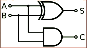
Figure 5. Half Adder Logic Diagram
As we know that NAND and NOR are called universal gates as any logic system can be implemented using these two, the half adder circuit can also be implemented using them. We know that a half adder circuit has one Ex – OR gate and one AND gate.
1.1)Half Adder using NAND gates
Five NAND gates are required in order to design a half adder. The circuit to realize half adder using NAND gates is shown below.
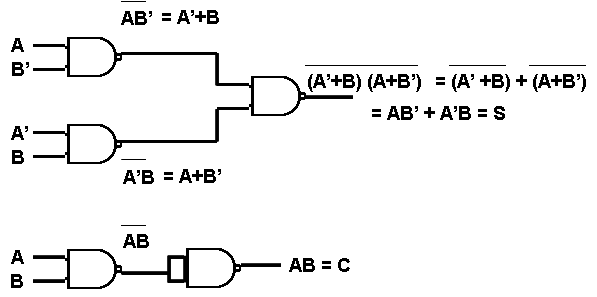
Figure 6. Realization of half adder using NAND gates
1.2)Half Adder using NOR gates
Five NOR gates are required in order to design a half adder. The circuit to realize half adder using NOR gates is shown below.
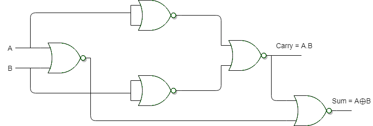
Figure 7. Realization of half adder using NOR Gates
Simulator 1:
- Step-1) Connect the supply(+5V)
 to the circuit.
 - Step-2) First press "ADD" button to add basic state of your output in the given table.
- Step-3) Press the switches to select the required inputs "A" and "B".
- Step-4) Press "ADD" button to add your inputs and outputs in the given table.
- Step-5) Repeat steps 3 & 4 for next state of inputs and their corresponding outputs.
- Step-6) Press the "PRINT" button after completing your simulation to get your results.
- Step-7) Press the "RESET" button whenever you want to refresh your simulator.
Simulator 2:
- Step-1) Enter the Boolean input "A" and "B".
- Step-2) Enter the Boolean output for your corresponding inputs.
- Step-3) Click on "Circuit" button to check the circuit diagram for half adder.
- Step-4) Click on "Check" Button to verify your output.
- Step-5) Click "Print" if you want to get print out of Truth Table.
- Step-6) Click on "Reset" button if you want to reset input and outputs.
LAB Simulation
2:- Full Adder
Full adder is a digital circuit used to calculate the sum of three binary bits. Full adders are complex and difficult to implement when compared to half adders. Two of the three bits are same as before which are A, the augend bit and B, the addend bit. The additional third bit is carry bit from the previous stage and is called 'Carry' – in generally represented by CIN. It calculates the sum of three bits along with the carry. The output carry is called Carry – out and is represented by Carry OUT.
The block diagram of a full adder with A, B and CIN as inputs and S, Carry OUT as outputs is shown below.
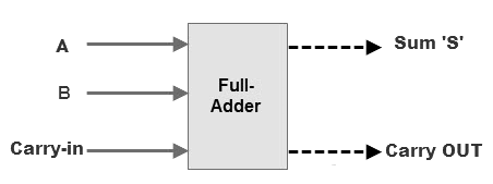
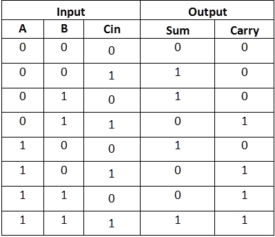
Figure 8. Full Adder Block Diagram and Truth Table
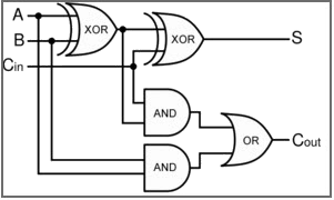
Figure 9. Full Adder Logic Diagram
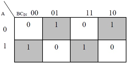
Based on the truth table, the Boolean functions for Sum (S) and Carry – out (COUT) can be derived using K – Map.
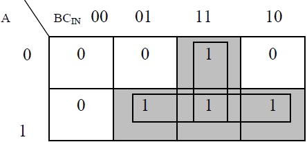
In order to implement a combinational circuit for full adder, it is clear from the equations derived above, that we need four 3-input AND gates and one 4-input OR gates for Sum and three 2-input AND gates and one 3-input OR gate for Carry – out.
2.1:- Full Adder using NAND gates
As mentioned earlier, a NAND gate is one of the universal gates and can be used to implement any logic design. The circuit of full adder using only NAND gates is shown below.
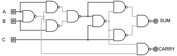
Figure 12. Full Adder using NAND gates
2.2)Full Adder using NOR gates
As mentioned earlier, a NOR gate is one of the universal gates and can be used to implement any logic design. The circuit of full adder using only NOR gates is shown below.
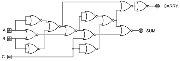
Figure 13. Full Adder using NOR gates
Simulator 1:
- Step-1) Connect the supply(+5V) to the circuit.
- Step-2) First press "ADD" button to add basic state of your output in the given table.
- Step-3) Press the switches to select the required inputs "A" and "B" and "Cin".
- Step-4) Press "ADD" button to add your inputs and outputs in the given table.
- Step-5) Repeat steps 3 & 4 for next state of inputs and their corresponding outputs.
- Step-6) Press the "PRINT" button after completing your simulation to get your results.
- Step-7) Press the "RESET" button whenever you want to refresh your simulator.
Simulator 2:
- Step-1) Enter the Boolean input "A" and "B" and "Cin".
- Step-2) Enter the Boolean output for your corresponding inputs.
- Step-3) Click on "Circuit" button to check the circuit diagram for full adder.
- Step-4) Click on "Check" Button to verify your output.
- Step-5) Click "Print" if you want to get print out of Truth Table.
- Step-6) Click on "Reset" button if you want to reset input and outputs.
LAB Simulation
Test
- William Gothmann H, Digital Electronics : An Introduction To Theory And Practice , Prentice Hall, 2nd ed. 1982
- M. Morris Mano, Michael D Ciletti, "Digital Design", Pearson, 4th ed. 2008
- Thomas L. Floyd, R. P. Jain, "Digital Fundamentals", Pearson, 11th ed. 2017
- S Salivahanan, S Arivazhagan, "Digital Circuits and Design", Vikas Publishing House Pvt Ltd., 3rd ed. 2009
- Ronald J. Tocci, Neal S. Widmer, Gregory L. Moss, "Digital Systems", Pearson, 10th ed. 2009
- Anil K. Maini, "Digital Electronics: Principles, Devices and Applications", Wiley-Blackwell, 2007
- Half Adder and Full Adder with Truth Table: https://www.elprocus.com/half-adder-and-full-adder/
- A half adder on breadboard: https://www.youtube.com/watch?v=OzGrf4CRVqg


Comments
Post a Comment