Experiments- 8
In Serial In Parallel Out (SIPO) shift registers, the data is stored into the register serially while it is retrieved from it in parallel-fashion. Figure 1 shows an n-bit synchronous SIPO shift register sensitive to positive edge of the clock pulse. Here the data word which is to be stored (Data in) is fed serially at the input of the first flip-flop (D1 of FF1). It is also seen that the inputs of all other flip-flops (except the first flip-flop FF1) are driven by the outputs of the preceding ones like the input of FF2 is driven by the output of FF1. In this kind of shift register, the data stored within the register is obtained as a parallel-output data word (Data out) at the individual output pins of the flip-flops (Q1 to Qn).
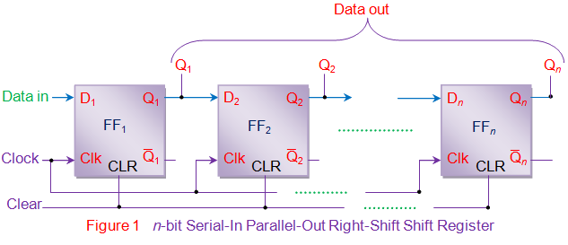
In general, the register contents are cleared by applying high on the clear pins of all the flip-flops at the initial stage. After this, the first bit, B1 of the input data word is fed at the D1 pin of FF1.This bit (B1) will enter into FF1, get stored and thereby appears at its output Q1 on the appearance of first leading edge of the clock. Further at the second clock pulse, the bit B1 right-shifts and gets stored into FF2 while appearing at its output pin Q2 while a new bit, B2 enters into FF1. Similarly at each clock pulse the data within the register moves towards right by a single bit while a new bit of the input word enters into the register. Meanwhile one can extract the bits stored within the register in parallel-fashion at the individual flip-flop outputs.
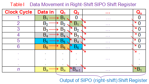
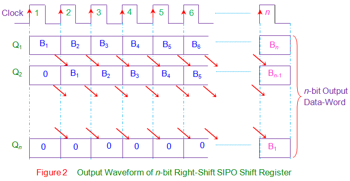
Analyzing on the same grounds, one can note that the n-bit input data word is obtained as an n-bit output data word from the shift register at the rising edge of the nth clock pulse. This working of the shift-register can be summarized as in Table I and the corresponding waveforms are given by figure 2.
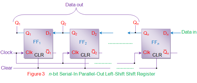
In the right-shift SIPO shift-register, data bits shift from left to right for each clock pulse. However if the data bits are made to shift from right to left in the same design, one gets a left-shift SIPO shift-register as shown by figure 3. Nevertheless the basic working principle remains the same except the fact that now Bn down to B1 is stored in Qn down to Q1 i.e. Q1 = B1, Q2 = B2 … Qn = Bn at the nth clock pulse.
Simulator :
- Step-1) Connect the supply(+5V)
 to the circuit.
 - Step-2) Keep the Reset and Preset as active-high signals
 .
. - Step-3) Apply the data at data input
 .
. - Step-4) Press clock pulse and observe this data at LED Q3.
- Step-5) Then press "ADD" button to add data in the given truth table.
- Step-6) Apply the next data at data input.
- Step-7) Press clock pulse and observe that the data at LED Q3will shift to LED Q2 and the new data applied will appear at Q3.
- Step-8) Repeat steps 3 to 5 till all the 4 bits appear at the output of shift register.
- Step-9) Press the "Print" button after completing your simulation to get your results.
LAB Simulation
Shift Registers
References
- William Gothmann H, Digital Electronics : An Introduction To Theory And Practice , Prentice Hall, 2nd ed. 1982
- M. Morris Mano, Michael D Ciletti, "Digital Design", Pearson, 4th ed. 2008
- Thomas L. Floyd, R. P. Jain, "Digital Fundamentals", Pearson, 11th ed. 2017
- S Salivahanan, S Arivazhagan, "Digital Circuits and Design", Vikas Publishing House Pvt Ltd., 3rd ed. 2009
- Ronald J. Tocci, Neal S. Widmer, Gregory L. Moss, "Digital Systems", Pearson, 10th ed. 2009
- Anil K. Maini, "Digital Electronics: Principles, Devices and Applications", Wiley-Blackwell, 2007
- Shift Register (SISO & SIPO Mode) using D Flip Flop: https://www.youtube.com/watch?v=OfoXcIymMvI
- Shift Register: https://www.electronics-tutorials.ws/sequential/seq_5.html
- Shift Registers: https://www.allaboutcircuits.com/textbook/digital/chpt-12/serial-in-parallel-out-shift-register/


Comments
Post a Comment