Carry Look-Ahead Adder
The motivation behind Carry Look-Ahead Adder :
In ripple carry adders, for each adder block, the two bits that are to be added are available instantly. However, each adder block waits for the carry to arrive from its previous block. So, it is not possible to generate the sum and carry of any block until the input carry is known. The  block waits for the
  block to produce its carry. So there will be a considerable time delay which is carry propagation delay.
Ripple Carry Adder-
- Ripple Carry Adder is a combinational logic circuit.
- It is used for the purpose of adding two n-bit binary numbers.
- It requires n full adders in its circuit for adding two n-bit binary numbers.
- It is also known as an n-bit parallel adder.
4-bit Ripple Carry Adder-
- A 4-bit ripple carry adder is used for the purpose of adding two 4-bit binary numbers.
- In Mathematics, any two 4-bit binary numbers A3A2A1A0 and B3B2B1B0 are added as shown below-

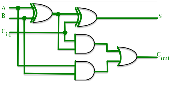
Using ripple carry adder, this addition is carried out as shown by the following logic diagram-

- Ripple Carry Adder works in different stages.
- Each full adder takes the carry-in as input and produces carry-out and sum bit as output.
- The carry-out produced by a full adder serves as carry-in for its adjacent most significant full adder.
- When carry-in becomes available to the full adder, it activates the full adder.
- After the full adder becomes activated, it comes into operation.
Consider the above 4-bit ripple carry adder. The sum  is produced by the corresponding full adder as soon as the input signals are applied to it. But the carry input
  is not available on its final steady-state value until carry
  is available at its steady-state value. Similarly depends on
  and on
  . Therefore, the carry must propagate to all the stages in order that output and carry settle their final steady-state value.
The propagation time is equal to the propagation delay of each adder block, multiplied by the number of adder blocks in the circuit. For example, if each full adder stage has a propagation delay of 20 nanoseconds, then will reach its final correct value after 60 (20 × 3) nanoseconds. The situation gets worse if we extend the number of stages for adding more bits.
Why Ripple Carry Adder is Called So?
In Ripple Carry Adder,
- The carry-out produced by each full adder serves as carry-in for its adjacent most significant full adder.
- Each carry bit ripples or waves into the next stage.
- That’s why it is called “Ripple Carry Adder”.
Disadvantages of Ripple Carry Adder-
- Ripple Carry Adder does not allow to use of all the full adders simultaneously.
- Each full adder has to necessarily wait until the carry bit becomes available from its adjacent full adder.
- This increases the propagation time.
- Due to this reason, the ripple carry adder becomes extremely slow.
- This is considered to be the biggest disadvantage of using a ripple carry adder.
Carry Look Ahead Adder-
A carry look-ahead adder reduces the propagation delay by introducing more complex hardware. In this design, the ripple carry design is suitably transformed such that the carry logic over fixed groups of bits of the adder is reduced to two-level logic.
- Carry Look Ahead Adder is an improved version of the ripple carry adder.
- It generates the carry-in of each full adder simultaneously without causing any delay.
- The time complexity of carry look-ahead adder
Logic Diagram-
The logic diagram for carry look-ahead adder is as shown below-

Carry Look Ahead Adder Working-
The carry-in of any stage full adder depends only on the following two parameters-
- Bits being added in the previous stages
- Carry-in provided in the beginning
Now,
- The above two parameters are always known from the beginning.
- So, the carry-in of any stage full adder can be evaluated at any instant of time.
- Thus, any full adder need not wait until its carry-in is generated by its previous stage full adder.
4-Bit Carry Look Ahead Adder-
- Consider two 4-bit binary numbers A3A2A1A0 and B3B2B1B0 are to be added.
- Mathematically, the two numbers will be added as-

From here, we have-
C1 = C0 (A0 ⊕ B0) + A0B0
C2 = C1 (A1 ⊕ B1) + A1B1
C3 = C2 (A2 ⊕ B2) + A2B2
C4 = C3 (A3 ⊕ B3) + A3B3
For simplicity, Let-
- Gi = AiBi where G is called carry generator
- Pi = Ai ⊕ Bi where P is called carry propagator
Then, re-writing the above equations, we have-
C1 = C0P0 + G0 ………….. (1)
C2 = C1P1 + G1 ………….. (2)
C3 = C2P2 + G2 ………….. (3)
C4 = C3P3 + G3 ………….. (4)
Now,
- Clearly, C1, C2 and C3 are intermediate carry bits.
- So, let’s remove C1, C2 and C3 from RHS of every equation.
- Substituting (1) in (2), we get C2 in terms of C0.
- Then, substituting (2) in (3), we get C3 in terms of C0 and so on.
Finally, we have the following equations-
- C1 = C0P0 + G0
- C2 = C0P0P1 + G0P1 + G1
- C3 = C0P0P1P2 + G0P1P2 + G1P2 + G2
- C4 =C0P0P1P2P3 + G0P1P2P3 + G1P2P3 + G2P3 + G3
These equations are important to remember.
These equations show that the carry-in of any stage full adder depends only on-
- Bits being added in the previous stages
- Carry bit which was provided at the beginning
Trick To Memorize Above Equations-
As an example, let us consider the equation for generating carry bit C2.
There are three possible reasons for the generation of C2 as depicted in the following picture-

In a similar manner, we can write other equations as well very easily.
Implementation Of Carry Generator Circuits-
The above carry generator circuits are usually implemented as-
- Two-level combinational circuits.
- Using AND and OR gates where gates are assumed to have any number of inputs.
Implementation Of C1–
- The carry generator circuit for C1 is implemented as shown below.
- It requires 1 AND gate and 1 OR gate.
C1 = C0P0 + G0

Implementation Of C2–
- The carry generator circuit for C2 is implemented as shown below.
- It requires 2 AND gates and 1 OR gate.
C2 = C0P0P1 + G0P1 + G1

Implementation Of C3 & C4–
Similarly, we implement C3 and C4.
- Implementation of C3 uses 3 AND gates and 1 OR gate.
- Implementation of C4 uses 4 AND gates and 1 OR gate.
Total number of gates required to implement carry generators (provided carry propagators Pi and carry generators Gi) are-
- Total number of AND gates required for addition of 4-bit numbers = 1 + 2 + 3 + 4 = 10.
- Total number of OR gates required for addition of 4-bit numbers = 1 + 1 + 1 + 1 = 4.

Circuit Diagram
The above equations are implemented using two-level combinational circuits along with AND, OR gates, where gates are assumed to have multiple inputs.
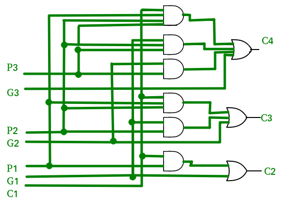
The Carry Look-ahead Adder circuit fro 4-bit is given below.

General Formula-
For an n-bit carry look-ahead adder to evaluate all the carry bits, it requires-
- Number of AND gates = n(n+1) / 2
- Number of OR gates = n

Advantages –
- The propagation delay is reduced.
- It generates the carry-in for each full adder simultaneously.
- It provides the fastest addition logic.
Disadvantages –
- The Carry Look-ahead adder circuit gets complicated as the number of variables increase.
- It involves complex hardware.
- The circuit is costlier as it involves more hardware.


Comments
Post a Comment