Construction of NOR gate latch and verification of its operation
Introduction
Latches are basic storage elements that operate with signal levels (rather than signal transitions). Latches controlled by a clock transition are flip-flops. Latches are edge-sensitive devices. Latches are useful for the design of the asynchronous sequential circuit.
SR (Set-Reset) Latch – SR Latch is a circuit with:
(i) 2 cross-coupled NOR gates or 2 cross-coupled NAND gates. (ii) 2 inputs S for SET and R for RESET. (iii) 2 outputs Q, Q.
The SR Latch using NOR gate is shown below with its truth table:
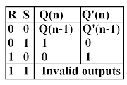
Figure-1:Logic Symbol of NOR gate latch Figure-2:Truth Table of NOR gate latch
While the R and S inputs are both low, feedback maintains the Q and Q outputs in a constant state, with Q the complement of Q. If S (Set) is pulsed high while R (Reset) is held low, then the Q output is forced high, and stays high when S returns to low; similarly, if R is pulsed high while S is held low, then the Q output is forced low, and stays low when R returns to low.The R = S = 1 combination is called a restricted combination or a forbidden state because, as both NOR gates then output zeros, it breaks the logical equation Q = Q. The combination is also inappropriate in circuits where both inputs may go low simultaneously (i.e. a transition from restricted to keep). The output would lock at either 1 or 0 depending on the propagation time relations between the gates (a race condition).
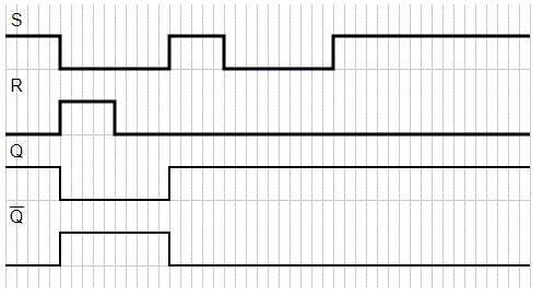
Figure-3:Timing Diagram of NOR gate latch
Simulator :
Step-1) Connect the supply(+5V) to the circuit.
Step-2) Press switch 1 for input R(Reset) and switch 2 for input S(Set).
Step-3) Then press "ADD" button to add data in the given truth table and simultaneously generate the timing diagram.
Step-4) Repeat step 2 and step 3 for another set of data.
Step-5) Press the "Print" button after completing your simulation to get your results.
Alternate Logic-Gate Representations We have discussed the five basic logic gates (AND, OR, INVERTER, NAND, and NOR) and the standard symbols used to represent them in a logic circuit diagram. Most of the logic networks use standard symbols. But in some networks an alternative set of symbols is used in addition to the standard symbols. The table shows the alternate set of symbols for the five basic gates. Table: Alternate Logic Gate Representations To convert any normal symbol to its corresponding alternate symbol, the following steps are used: METHODOLOGY: TO CONVERT STANDARD SYMBOL TO ALTERNATE SYMBOL Step 1: Add bubbles (indication of inversion) at those input or output points where it is not present. Step 2: Remove all pre-existing bubbles of the normal symbol, if there is any at the point (only NOT, NAND and NOR gates) Step 3: If the existing normal logic symbol is AND, change it to OR, Similarly, if it is OR, then change it to AND. There is no change for the triangular symbol of ...
Definition: The algebra of logic is a Boolean algebra. It works with variables with two different values, such as 0 (False) and 1 (True), as well as logically significant operations. George Boole invented the first way of manipulating symbolic logic, which later became known as Boolean Algebra. Because of its vast applications in switching theory, developing basic electronic circuits, and designing digital computers, Boolean algebra has become a vital tool in computer science. The following are the basic operations of Boolean algebra: AND or conjunction operation OR operation or disjunction Not or Negative operation Rules: Suppose X and Y are two Boolean variables, then the three operations are defined as follows; X AND Y, satisfies X ∧ Y = True, if X = Y = True or else X ∧ Y = False. X OR Y, satisfies X ∨ Y = False, if X = Y = False, else X ∨ Y = True. ¬X satisfies ¬X = False, if X = True and ¬X = True if X = False Boolean Algebra Questions with Solutions 1. Define Boolean expression....

 to the circuit.
 for input R(Reset) and switch 2

Comments
Post a Comment